TL-WR841 RAM/ROM Upgrade
(Tutorial for TP-Link TL-WR841N(D) v8,v9,v10,v11,v12)
With the next release of OpenWRT (>19.07.3) no images for devices only containing 4Mbyte flash and 32Mbyte RAM will be build. So devices like the TP-Link TL-WR841N will get no future images. But luckily the popular TP-Link TL-WR841N can be fairly easily upgraded, provided one is able to solder smd components, and building your own image is no magic.
Starting with 19.07.0 OpenWRT switched TL-WR841N from target ar71xx into the new ath79 target. Due to Flash size limitation all pre-build images do not contain a webinterface. To make flashing easier after switching to a new ROM chip, we will initially use a 18.0x.x build with included webinterface. After building our own fresh image including a webinterface and a more recent linux kernel we can flash it with no problems afterwards.
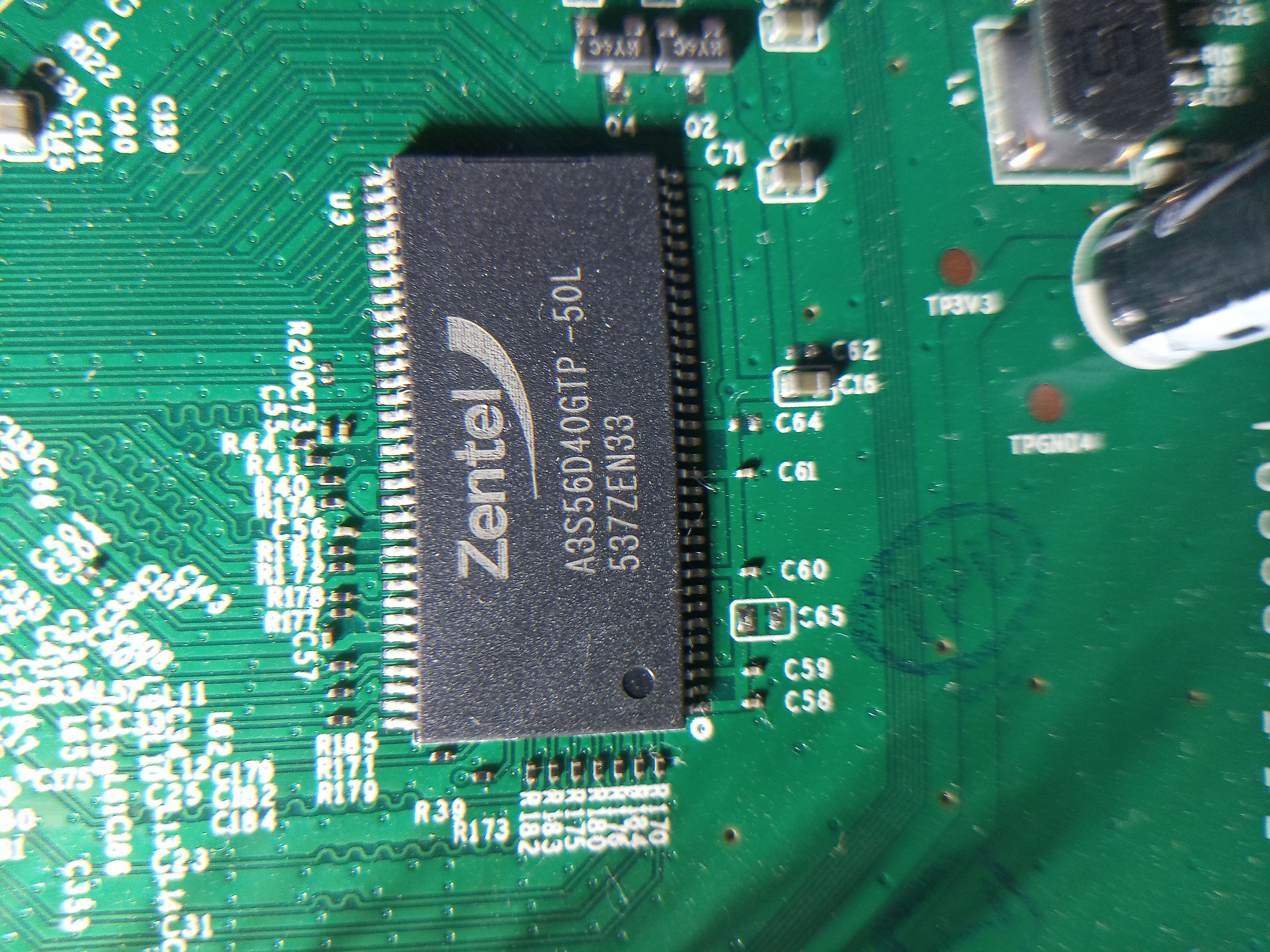
The most difficult part is the RAM upgrade, because the TSOP-II 66pin chip is not the easiest to desolder. I’ve done my swap with the help of a hot-air station. This step may be optional but without, OpenWRT will easily run out ouf RAM and you may be very limited functionality wise.
Swapping the ROM chip is not to difficult. A hot-air station may make the process a breeze, but using only a soldering iron is barely harder.
Helpful tools for soldering are a pair of small tweezers, solder, flux, and solder-wick.
Prequisites:
| 64Mbyte RAM chip -> optional but recommended |
| 8/16Mbyte flash chip |
| flash programmer |
| Linux (Windows possible by using cygwin) |
for possible RAM and ROM chips look at the bottom tables.
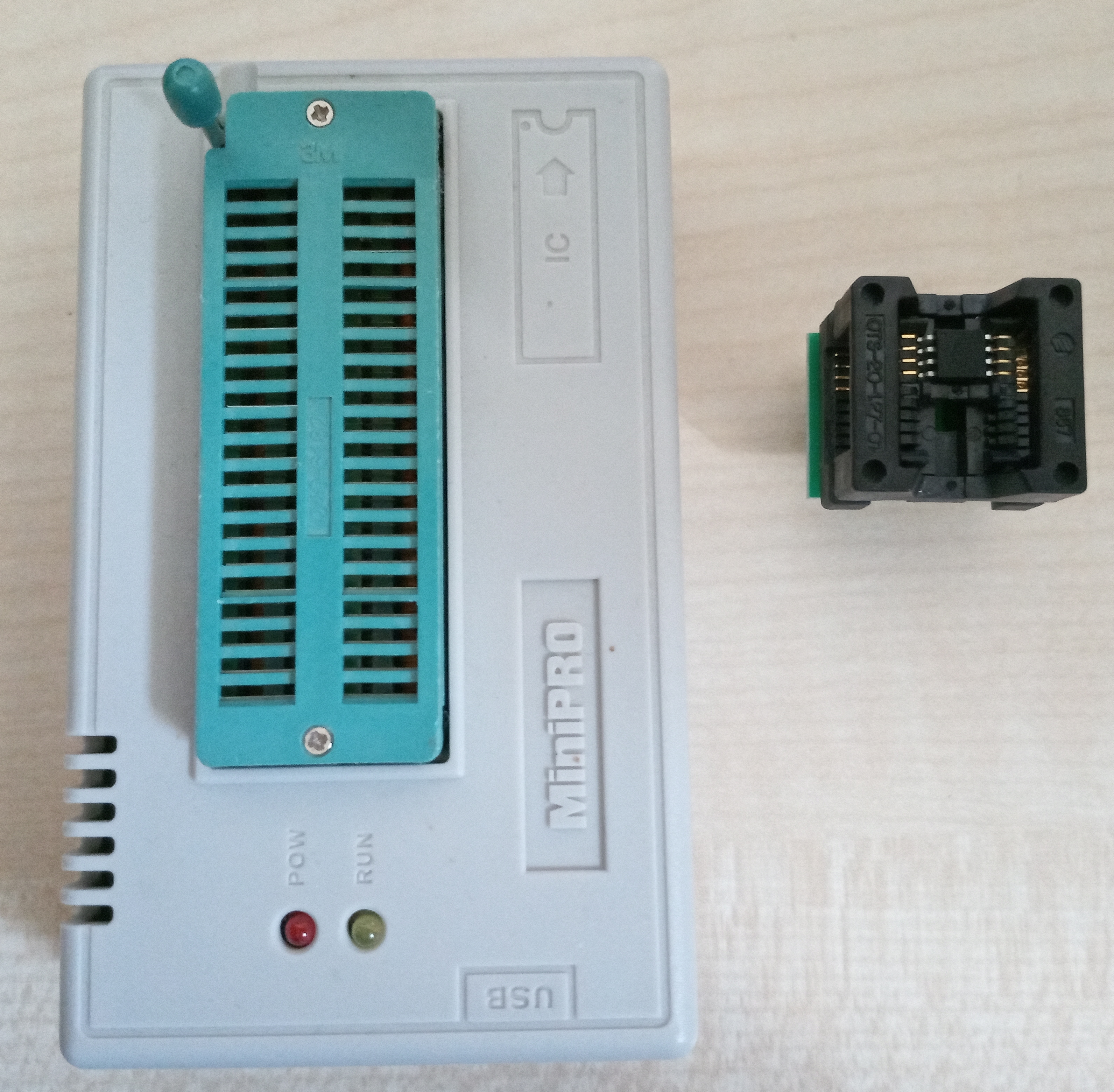
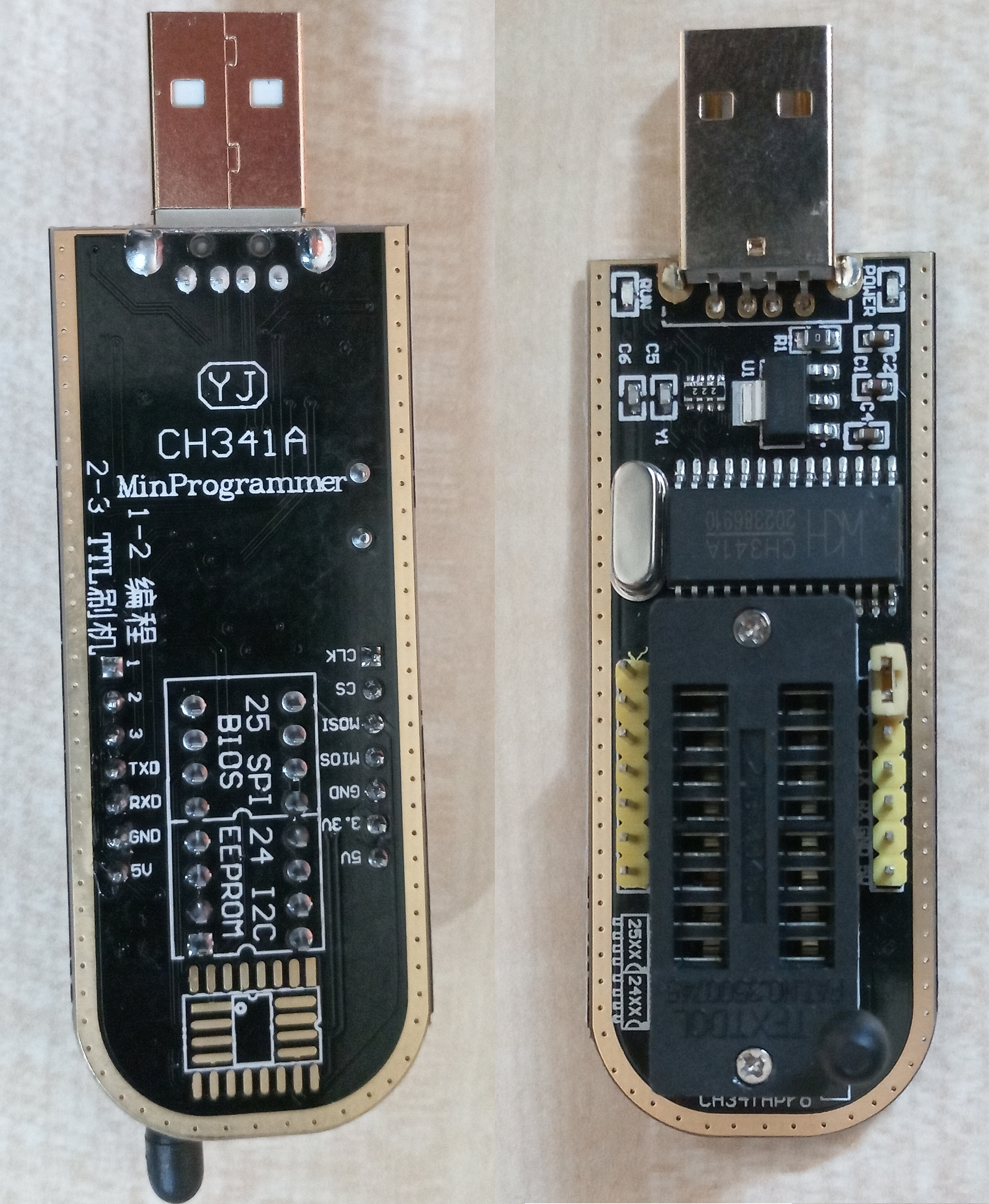
to read the old flash chip and write the new one, a flash programmer is needed. I used the TL866CS MiniPro. There are plenty of options for flash programmer, like the CH341A (popular for BIOS flashing) and you can easily use a raspberry pi (just search for raspberry pi SPI flasher).
×Warning! Doing upgrades step by step, will help troubleshooting in case of problems. Do either ROM or RAM first and check before progressing
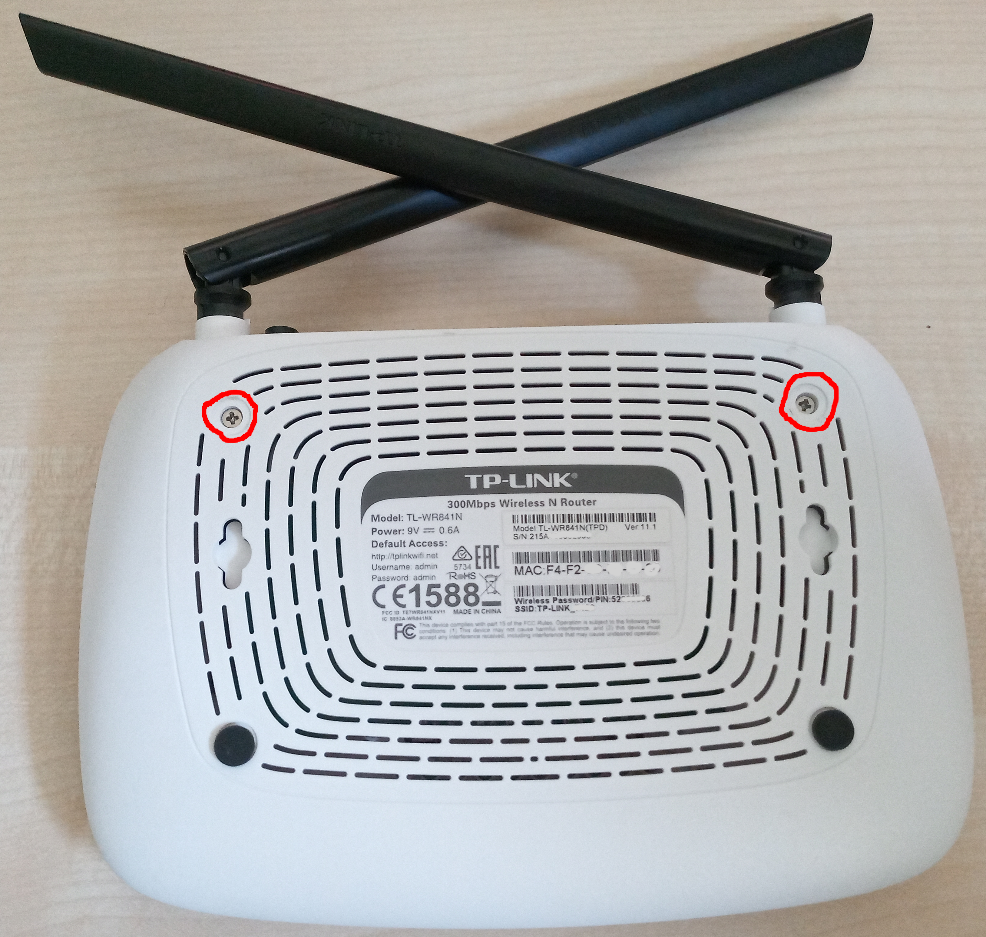
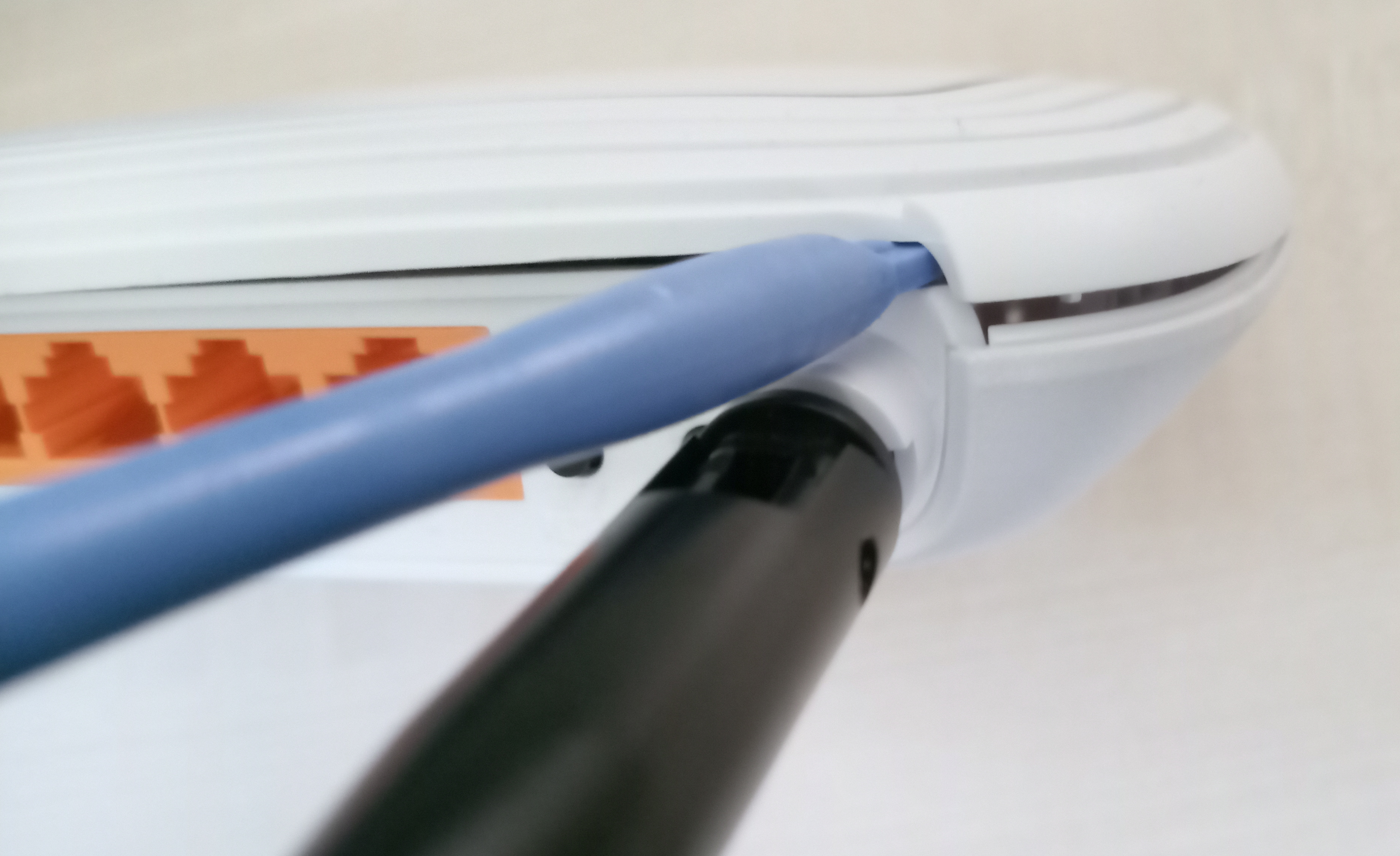
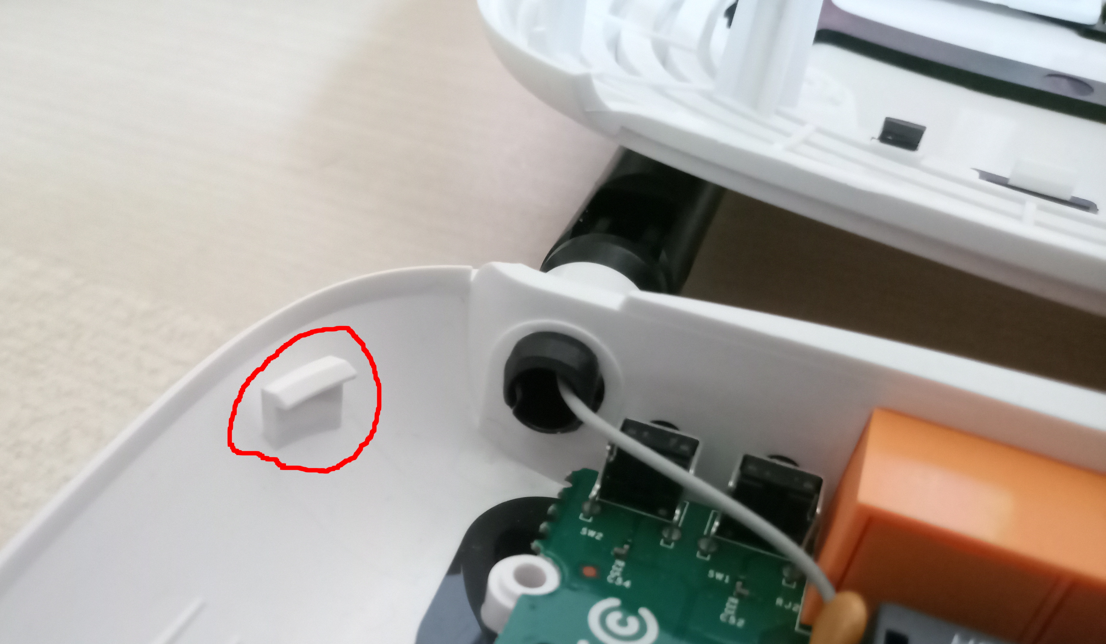
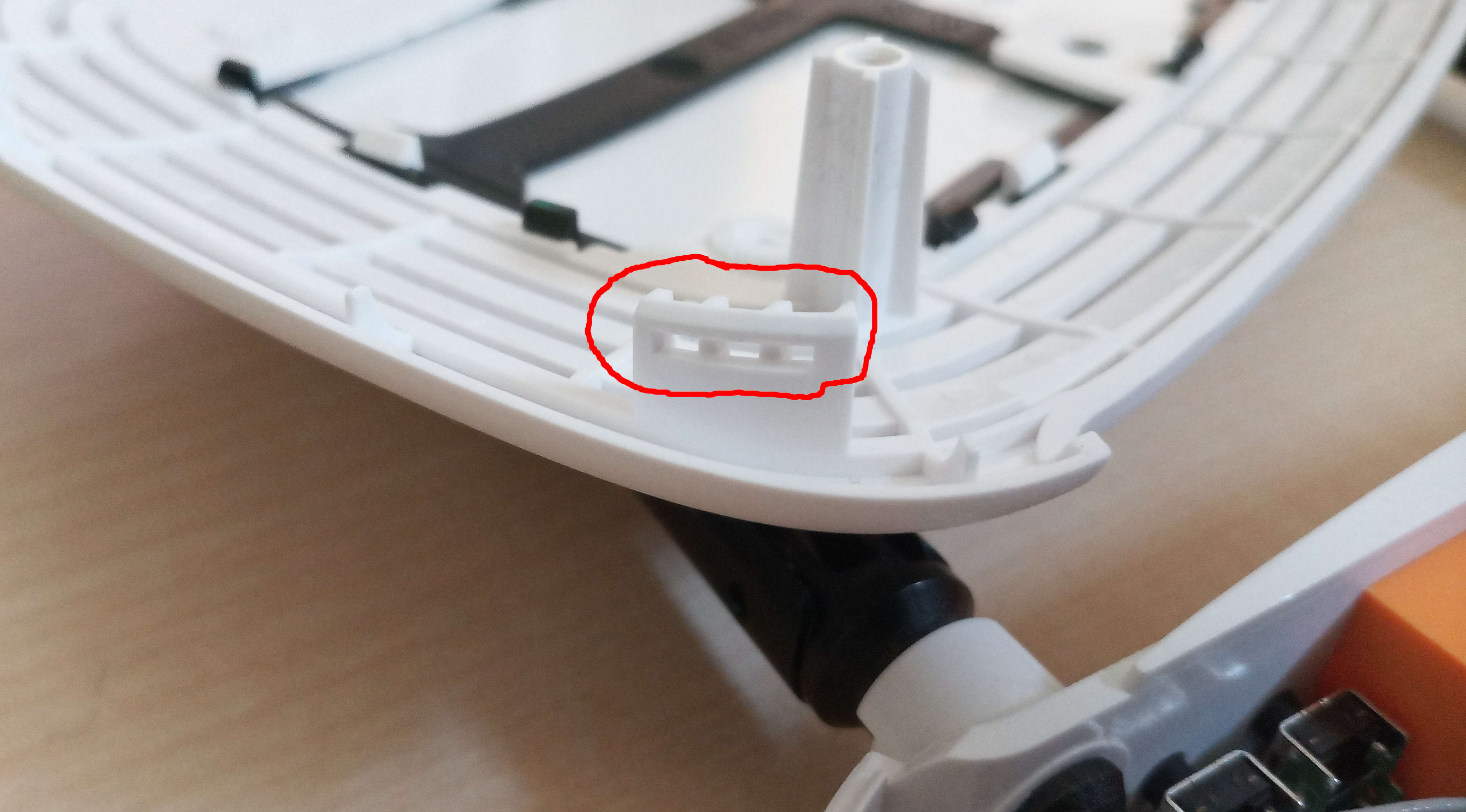
Open Device

RAM
to upgrade RAM only swapping of the RAM chip has to be done.
×Warning! Be careful to not knock of any small components around the RAM chip or damage any traces or pads. Doing so will most probably render your device inoperable.
the best method (in my opinion) to remove the old chip, is by using a hot-air station with flux. But if you don’t care about the old RAM chip surviving you can take a box cutting knife and carefully cut off the legs as close as possible to the chip. Do not cut into the PCB by doing so. The remaining legs on the board can be removed with a normal solderin iron one by one.
After the chip is removed, use some flux and solder wick to clean of the solder pads.
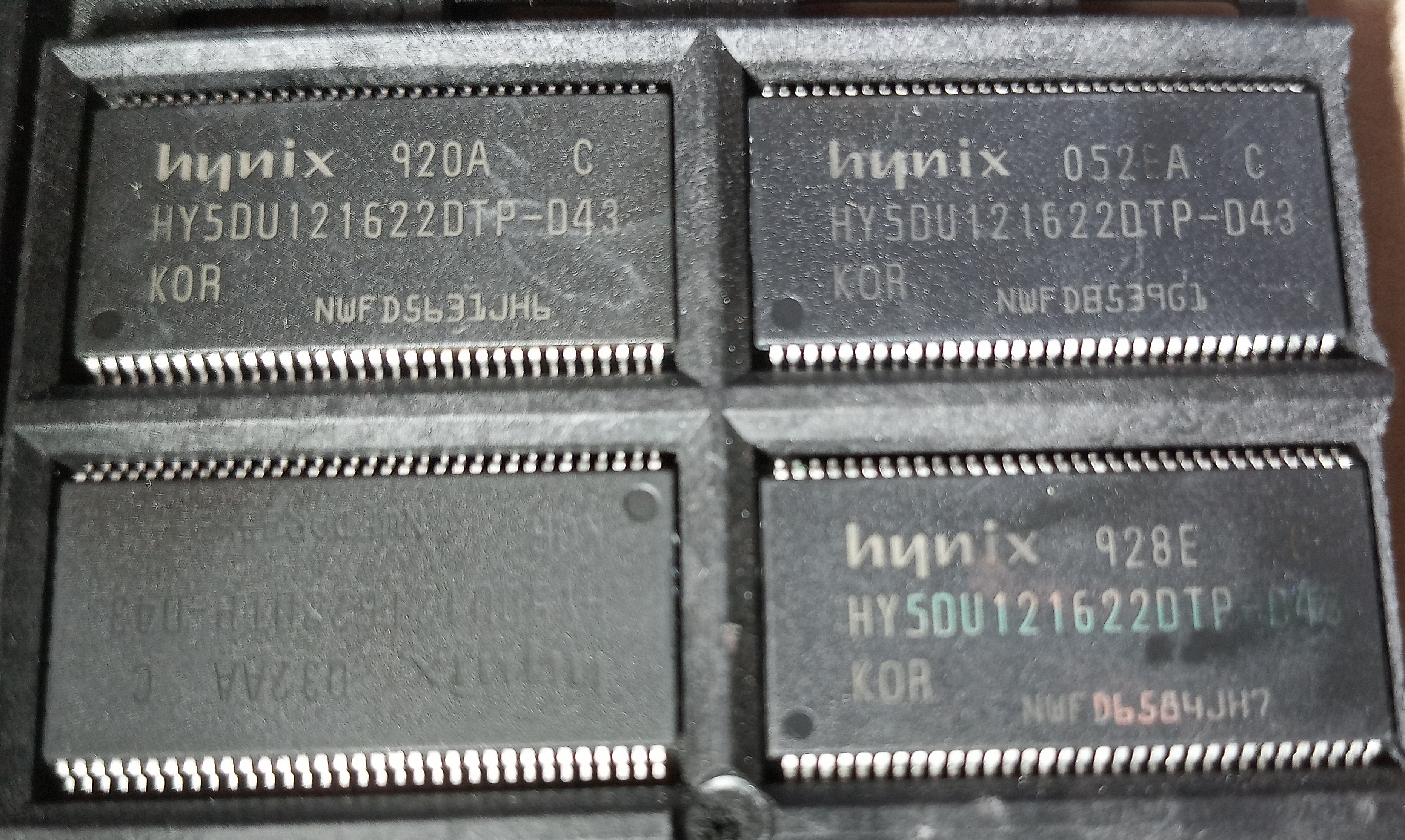
Place the new RAM chip in the right orientation (white mark on board corresponds to indent on chip) on the pads. First only solder one of the corner legs to align and stabilize the chip. Next solder the corner on the opposite site before you can solder the rest.
If all went good the new RAM will be automaticly detected by the Processor and the device will start just fine. It can also be checked on the Overview in luci webinterface or via ssh.
ROM
As the first step we need a dump of the original ROM to extract the ART-partition (Atheros Radio Test). Without this the wireless will not work.

To dump the rom, remove the chip and put it in a flash programmer. Due to the necessity of flash programmer for writing new chip anyway, dumping through ssh when OpenWRT is already running on device is not scope of this tutorial.

Also a raspberry pi can be used as a SPI flash programmer needing basicly only a couple wires.
| Flash ROM | Raspberry Pi |
|---|---|
| !SS (1) | GPIO8 (SPI0_CED_N) |
| MISO (2) | GPIO9 (SPI0_MISO |
| !WP (3) | 3V3 |
| GND (4) | GND |
| MOSI (5) | GPIO10 (SPI0_MOSI) |
| SCK (6) | GPIO11 (SPI0_SCLK) |
| !HOLD (8) | 3V3 |
| VDD (8) | 3V3 |
×Information: This tutorial does not show how to use a specific programmer. Focus lies on TL-WR841N specific parts.
Create new flash image
By just copying the old ROM to a bigger flash chip won’t work because of the partition layout needed for booting the device. The ART-partition has to be at the end of the flash rom and by simply copying it would end up somewhere in the middle. So the first step is to extract this partition. Also the original firmware will not work anymore.
To prevent an unbootable device we also change the bootloader to u-boot-mod to get best compatability with a range of flash chips and very good firmware recovery options.
the last 64 Kbyte of the dump contains the ART-partition. to extract it:
dd ibs=4k skip=1008 if=dump.bin of=art.bincreate an zero filled dummy out.bin file with the size of the new flash chip
dd if=/dev/zero ibs=4k count=4096 | tr "\000" "\377" > out.bin
#for 8MB chips use 2048 instead of 4096
copy ART-partition to the end of out.bin
dd conv=notrunc obs=4k seek=4080 if=art.bin of=out.bin
#for 8MB chips use 2032 instead of 4080
download bootloader version for your device (for v12 use v11 uboot) and copy it to the beginning of out.bin
dd conv=notrunc if=tp-link-tl-wr841n-vVERSION.bin of=out.bin
#replace VERSION with your device version
download OpenWRT image for your device (tl-wr841-vVERSION-squashfs-sysupgrade.bin). Every release version <19.0x.x will suffice as we will upgrade to newer ath79 target image later. Afterwards we copy it into the out.bin behind the bootloader.
dd conv=notrunc obs=4k seek=32 if=tl-wr841-vVERSION-squashfs-sysupgrade.bin of=out.bin
#replace VERSION with your device version
for proper operation the MAC address and version string has to be written inside the image.
×Warning! Not setting the correct version string will lead to problems with flashing firmware later on
printf '\xAA\xBB\xCC\xDD\xEE\xFF' | dd conv=notrunc ibs=1 obs=256 seek=508 count=6 of=out.bin
#replace AA BB CC DD EE FF with MAC address on bottom label of device
printf '\x08\x41\x00\xVERSION\x00\x00\x00\x01' | dd conv=notrunc ibs=1 obs=256 seek=509 count=8 of=out.bin
#replace VERSION with your device version written with leading 0 if only one letter (e.g. \xVERSION -> \x09 for v9)
now the out.bin image is ready to be flashed to the new chip. Afterwards it can be soldered in place of the old chip and the device is ready to be booted.
Pre-builtd images
× pre-built images for 16M v11 and v12 can be found in the following link
Building newest version with webinterface
for dependencies necessary to build own image refer to official site
following steps should NOT be done as ‘root’ or with ‘sudo’
clone OpenWRT git repository
git clone https://git.openwrt.org/openwrt/openwrt.git openwrtchange into the openwrt directory
cd openwrtupdate and install feeds (e.g. needed for luci webinterface)
./scripts/feeds update -a
./scripts/feeds install -a
at this point an adjustment to some source files is necessary to build an image using the new flash size. edit following files:
target/linux/ath79/dts/qca9533_tplink_tl-wr841.dtsi
in this part the addresses must be adjusted for 8/16M flash size
flash@0 {
		compatible = "jedec,spi-nor";
		reg = <0>;
		spi-max-frequency = <25000000>;

		partitions {
			compatible = "fixed-partitions";
			#address-cells = <1>;
			#size-cells = <1>;

			uboot: partition@0 {
				label = "u-boot";
				reg = <0x000000 0x020000>;
				read-only;
			};

			partition@20000 {
				compatible = "tplink,firmware";
				label = "firmware";
				reg = <0x020000 0x3d0000>;
			};

			art: partition@3f0000 {
				label = "art";
				reg = <0x3f0000 0x010000>;
				read-only;
			};
		};
here are the finished changes
flash@0 {
		compatible = "jedec,spi-nor";
		reg = <0>;
		spi-max-frequency = <25000000>;

		partitions {
			compatible = "fixed-partitions";
			#address-cells = <1>;
			#size-cells = <1>;

			uboot: partition@0 {
				label = "u-boot";
				reg = <0x000000 0x020000>;
				read-only;
			};

			partition@20000 {
				compatible = "tplink,firmware";
				label = "firmware";
				reg = <0x020000 0xfd0000>; //for 8M use 0xfa0000 instead of 0xfd0000
			};

			art: partition@ff0000 {       //for 8M use fc0000 instead of ff0000
				label = "art";
				reg = <0xff0000 0x010000>; //for 8M use 0xfc0000 instead of 0xff0000
				read-only;
			};
		};
target/linux/ath79/image/tiny-tp-link.mk
find your tplink-tl-wr841-vXX version and alter 4mlzma for the new flash size. example shows passage for TL-WR841 v11. This looks similar for all other versions.
define Device/tplink_tl-wr841-v11
  $(Device/tplink-4mlzma)
  SOC := qca9533
  DEVICE_MODEL := TL-WR841N/ND
  DEVICE_VARIANT := v11
  TPLINK_HWID := 0x08410011
  SUPPORTED_DEVICES += tl-wr841n-v11
  IMAGES += factory-us.bin factory-eu.bin
  IMAGE/factory-us.bin := tplink-v1-image factory -C US
  IMAGE/factory-eu.bin := tplink-v1-image factory -C EU
endef
TARGET_DEVICES += tplink_tl-wr841-v11
in this example the necessary change made to TL-WR841 v11 is shown, but it’s basically the same for all other versions, just alter there description part of the file.
define Device/tplink_tl-wr841-v11
  $(Device/tplink-16mlzma)    //for 8M use tplink-8mlzma instead of tplink-16mlzma
  SOC := qca9533
  DEVICE_MODEL := TL-WR841N/ND
  DEVICE_VARIANT := v11
  TPLINK_HWID := 0x08410011
  SUPPORTED_DEVICES += tl-wr841n-v11
  IMAGES += factory-us.bin factory-eu.bin
  IMAGE/factory-us.bin := tplink-v1-image factory -C US
  IMAGE/factory-eu.bin := tplink-v1-image factory -C EU
endef
TARGET_DEVICES += tplink_tl-wr841-v11
at the next step we will configure the build script to build a image for our device
make menuconfig| ‘Target System’ -> ‘Atheros ATH79 (DTS) |
| ‘Subtarget’ -> ‘Devices with small flash’ |
| ‘Target Profile’ -> ‘TP-Link TL-WR841N/ND vVERSION’ (choose your device VERSION here) |
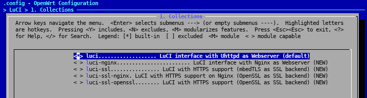
| ‘LuCI’ -> ‘Collections’ -> <*> ‘luci’ (make sure to mark with * not with M) |
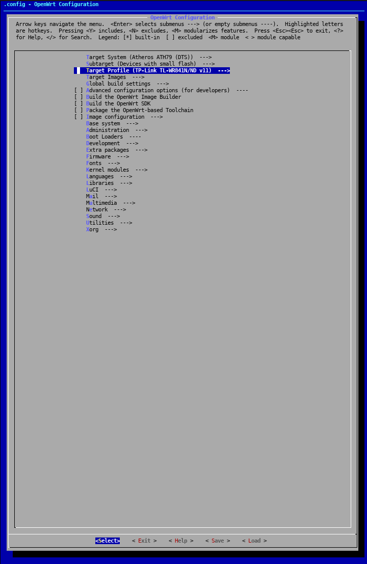
afterwards choose exit and save when you are asked
let the build system download all missing files
make downloadstart build
makethe finished image will be in following folder bin/targets/ath79/tiny/
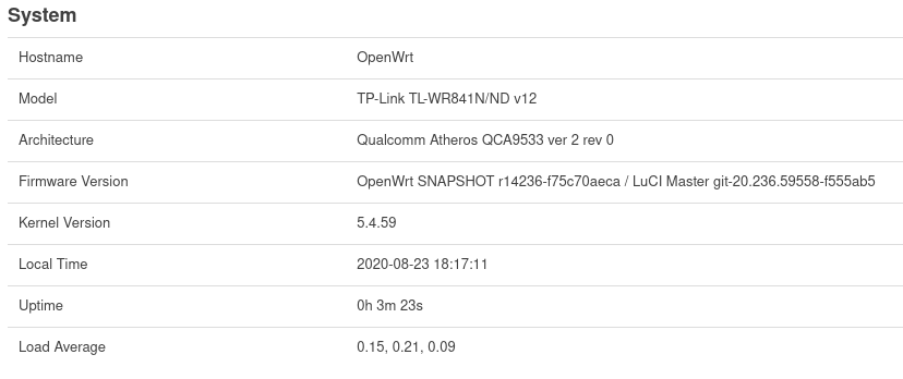
this can now be flashed via the webinterface
×Warning! Settings can NOT be kept because of the switch from *ar71xx* to *ath79*. Keeping the settings will lead to a boot loop and a recovery method will be necessary
Recovey method with new uboot
by holding the reset button for 3-4sec after powering on the device, it will start a recovery webinterface with the IP: 192.168.1.1
Possible chips
This list only shows examples and is by no means exhaustive. All similar chips, meeting the specifications should work.
RAM (64MByte/512MBit DDR1 32Mx16 TSOP-II 66pin)
| Hynix HY5DU121622CTP-D43 -> used in this tutorial |
| Samsung K4H511638B-TCB3 |
| Samsung K4H511638D-UCB3 |
| Elpida D5116AFTA-5B-E |
ROM (3/3.3V 128/64MBit Serial Flash SOIC8)
| Winbond W25Q64 (8MB) |
| Winbond W25Q128 (16MB) -> used in this tutorial |
| Spansion S25FL064P (8MB) |
| Spansion S25FL127S (16MB) |
Downloads:
| 16M_builds |
| bootloader |
| OpenWRT image |
| u-boot-mod |